LankeCMS LOGO
Featured Products
Silicon Wafer
View Detailed
SOI Wafer
View Detailed
SiO2 Wafer
View Detailed
TiO2
View Detailed
GaSb Wafer
View Detailed
InSb Wafer
View Detailed
sapphire substrate
View Detailed
Ge Wafer
View Detailed
Filter
View Detailed
PRODUCTS LIST Home > Product Show
Silicon Wafer

Product Numbers: JAH-Si Wafer

Place:

Product description:Silicon Wafer,Silicon Wafer factory,Grind Wafer, Single side polishing,Double side polishing,IC grade silicon wafer

INTRODUCTION

 Product Specification


Outline Size:

2"; 3"; 4"; 6"; 812"

Customize

Type:

N Type or P Type or Intrinsic

Customize

Diameter:

50-300mm

Thickness:

200 -1000 μm

Customize

Thickness Deviation:

±10μm

Total Indicated Runout(TIR):

< 3 μm

BOW

≤15μm

TTV:

≤10μm

Resistivity:

0.0001-10000 (Ω·cm)

Customize

Carbon content:

≤5.0 × 10¹⁶ atoms/cc

Oxygen content:

≤1.0 ×10¹⁸ atoms/cc

Crystal Orientation:

100± 2;〈110± 2;〈111± 2

Customize

Minority carrier lifetime:

≥15μs

Dislocation density

3X10³ /cm2

Grade:

Optical or Solar or IC

Customize

Surface Treatment:

Lapping, Single Side Polishing, Double Side Polishing

Customize


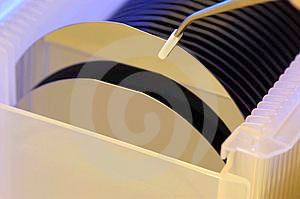
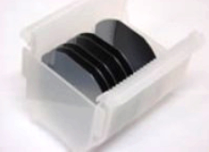
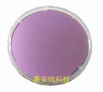
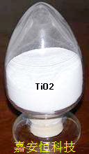
Please indicate the information as below if you want to buy this product

1、Resistivity;

2、Size;

3、Thickness

4、Single Side Polishing or Double Side Polishing or Grind

5、Grade

6、Conduction type: P Type or Ntype or Intrinsic

7、Doping type:Doping B,Doping P,Doping As,Doping Ga,Doping Sb,or Doping None

8、Quantity

Links:Instrument  |   9Hui Tech  |   semi  |   coema  |   Background Management  |  
  Beijing Jiaanheng All rights reserved  京ICP备12052793号
  Add:Beijing China Tel:010-88681435 Fax:010-58872911