|
|
|
PRODUCTS LIST
Home > Product Show
|
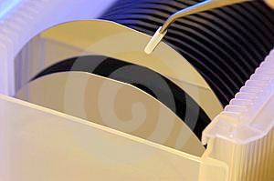
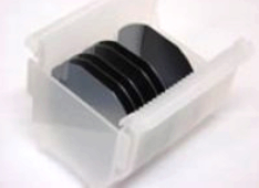
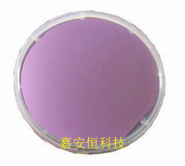
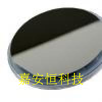
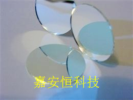
sapphire substrate
Product Numbers: 2012121372342
Place:
Product description:sapphire substrate,sapphire substrate factory

|
|
|
INTRODUCTION
Product Specification
|
Crystal Materials
|
99,996% of Al2O3,High Purity, Monocrystalline, Al2O3
|
|
|
Crystal quality
|
Inclusions, block marks, twins, Color, micro-bubbles and dispersal centers are non-existent
|
|
|
Diameter
|
2inch
|
3inch
|
4inch
|
5inch ~ 7inch
|
|
|
50.8± 0.1mm
|
76.2±0.2mm
|
100±0.3mm
|
In accordance with the provisions of standard production
|
|
|
|
Thickness
|
430±15µm
|
550±15µm
|
650±20µm
|
In accordance with the provisions of standard production
|
|
|
330±15µm
|
500±15µm
|
550±20µm
|
|
|
250±15µm
|
430±15µm
|
500±20µm
|
|
|
Orientation
|
C- plane (0001) to M-plane (1-100) or A-plane(1 1-2 0) 0.2±0.1° /0.3±0.1°, R-plane (1-1 0 2), A-plane (1 1-2 0 ), M-plane(1-1 0 0), Any Orientation , Any angle
|
|
|
Primary flat length
|
16.0±0.8mm
|
22.0±1.0 mm
|
32.5±1.5 mm
|
In accordance with the provisions of standard production
|
|
|
Primary flat Orientation
|
A-plane (1 1-2 0 ) ± 0.2°
|
|
|
TTV
|
≤10µm
|
≤15µm
|
≤20µm
|
≤30µm
|
|
|
LTV
|
≤10µm
|
≤15µm
|
≤20µm
|
≤30µm
|
|
|
TIR
|
≤10µm
|
≤15µm
|
≤20µm
|
≤30µm
|
|
|
BOW
|
≤10µm
|
≤15µm
|
≤20µm
|
≤30µm
|
|
|
Warp
|
≤10µm
|
≤15µm
|
≤20µm
|
≤30µm
|
|
|
Front Surface
|
Epi-Polished (Ra< 0.2nm)
|
|
|
Back Surface
|
Fine ground (Ra=0.5 to 1.2 µm), Epi-Polished (Ra< 0.2nm)
|
|
|
Note
|
Can provide high-quality sapphire substrate wafer according to customers' specific requirement
|
|
|