|
Crystal Material
|
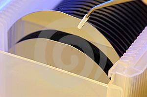
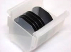
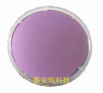
Single Crystal Gallium Arsenide, VGF / LECgrown, 高纯单晶
|
|
Crystal Orientation
|
(1 0 0) / (1 1 1)
|
|
Doping
|
Undoped
|
Zn
|
Si / Te
|
|
Diameter
|
50~150mm ± 0.25mm(2"、 3"、 4"、6")
|
|
Thickness
|
350 ± 25um / 550 ± 25um / 625 ± 25um
|
| Crystal Orientation Angle
|
( 100 )or(111) α 0 ±β 0, off angle α and accuracy β upon request
|
|
Resistivity
|
(1-30)x10 7 Ω.cm
|
(1-10)x10 -3 Ω.cm
|
|
Mobility Ratio
|
1500~3000 3000~5000 cm2 / V·sec
|
N / A
|
|
doping content
|
N / A
|
(0.1-3.0)×10 18 /cm3
|
|
Etch Pit Density
|
≤ 5·103 cm-2
|
≤ 7·10 4cm-2
|
≤ 5·102 cm-2
|
| Primary flat length
|
(0-1-1)±0.5deg, 16 ±1.0mm /22±1.0mm/32.5±1.0mm
|
| Second flat length
|
(0-1 1) )±5.0 deg, 8 ±1.0mm / 11±1.0mm/ 18±1.0mm
|
|
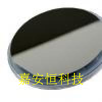
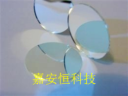
Front surface
|
Polished in Epi-ready Prime grade, 外延生长级抛光
|
|
Back Surface
|
Polished / Lapping or Etched, 抛光 / 研磨或腐蚀
|
|
Epi-ready
|
Yes
|